Development
To develop on Louvre board are required:
- Software:
- LPCXpresso
- Application firmware project, compatible with bootloadaer
- Bootloader firmware project
- Hardware:
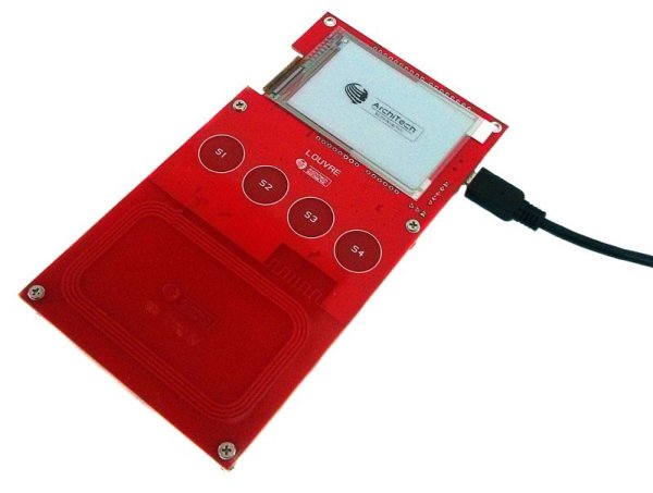
- Louvre Board
- NXP LPC-Link (version 1 or 2), please refer to embeddedartists website. In this guide we have tested both the LPC-Link 1 of this board and the LPC-Link 2.
Download LPCExpresso
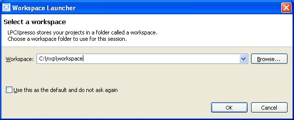
The developement software used is LPCxpresso, we suggest to install at the least version 7.3. This application is freely downloadable from lpcware site. Go to lpcxpresso webpage Install the LPCxpresso following default procedure. In this guide the SDK is installed in the default path C:\nxp and we refer to this in our example. After the installation you need to register in order to activate the Free Edition of the LPCXpresso. Launch the SDK selecting as workspace folder C:\nxp\workspace.
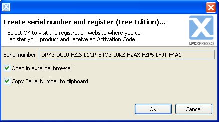
Select from menu Help -> Activate -> Create serial number and register (Free Edition). Check the options Open in external browser and Copy Serial Number to clipboard then press Ok button.
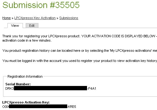
From the website you need to register and insert the serial number. It will display your activation code.
The activation code must be inserted into the window-form selectionable from the menu Help -> Activate -> Activate (Free Edition)
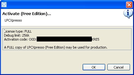
If all is done correctly now you are able to deploy with the Free Edition LPCXpresso, permitting you to debug up to 256KB.
Firmware Projects
To get the last source of the firmware and bootloader, go to architechboards website. This site provides software and documentation needed to develop with the Louvre board. Save it in your bookmarks to be updated with the new releases. In the homepage select the Louvre board in the Products menu.
Application Firmware
This is the software which permits to the Louvre to retrieve the images on the Louvre board via the Android application called Louvre Image Sender and run the Power Mode interface.
Import Application Project
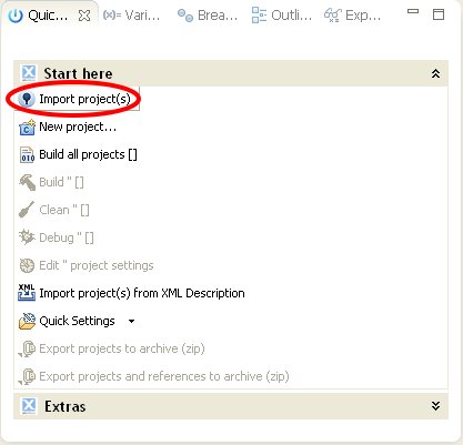
You can import the project directly from the packed file downloaded before. In order to do this, press on Import Project:
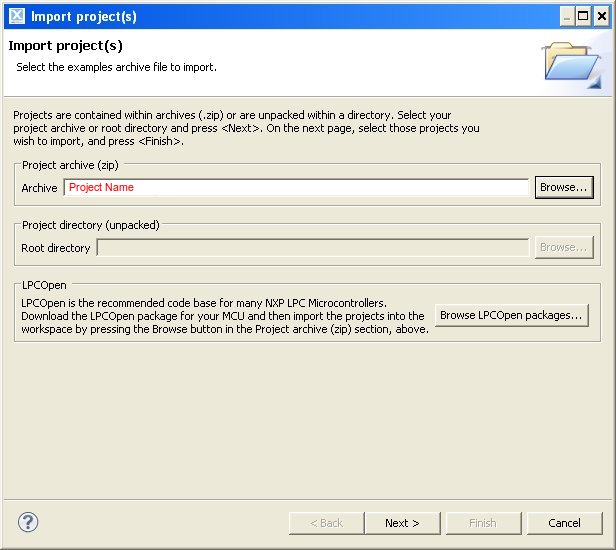
Then browse and select the ArchiTech_Louvre_Firmware.zip file, click on next button:
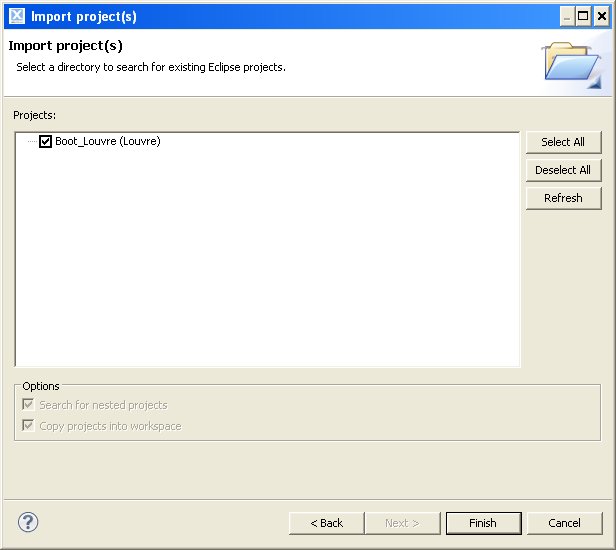
Select all and click another time on next button:
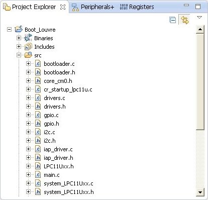
Now you have the project loaded:
Project files will be moved under the workspace directory.
Download into Louvre
In order to download the firmware into Louvre board you have to:
1. Recompile the Louvre Firmware Update Android application with the firmware.hex file built previously. You can find the source project on github. To change the downloaded firmware, the file firmware.hex must be changed under the this folder.
- Use the Louvre Firmware Update to upload the Louvre board.
Note
It is not possible debug the application due the relocation memory in order to be compatible with the bootloader firmware.
Firmware Details
All libreries code used is been imported directly into the project: i2c.c, ssp.c, gpio.c, timer.c and adc.c. The file adc.c is not used.The code for the e-paper is in the modules eink.c and fonts.c.The module driver.c is for manage temperature sensor, capacitive buttons and nfc protocol.To have more details, the source code is provided with comments.
Bootloader Firmware
This is the software which permits to the Louvre to retrieve a newer Application Firmware via the Android application called Louvre Firmware Update.
Import Bootloader Project
You can import the project directly from the packed file downloaded before. In order to do this, press on Import Project:
Then browse and select the ArchiTech_Louvre_Boot_Firmware.zip file, click on next button:
Select all and click another time on next button:
Now you have the project loaded:
Project files will be moved under the workspace directory.
Important
Download into Louvre
Once you have compiled the project you have the firmware.bin file outupt into debug folder. To upload it in the Louvre board you have two choice. The first, the easiest is with mini-USB cable:
- Check the jumper CN4 is setted correctly:
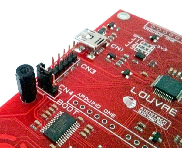
- it’s insert mini-usb cable from PC to the CN1 connector of the board.
- The PC will see the Louvre board as a storage memory, delete the old firmware.bin file and copy the newer firmware.bin file into the mass storage.
The second choice is using the LPC-Link 1 or LPC-Link 2:
- LPC-Link 1
1. make sure that you have connected the LPC-Link to PC. Connect with a cable the J4 LPC-Link connector to the CN3 connector of the Louvre board. Here the connection scheme:
| pin J4 | pin CN3 | Signal Names |
|---|---|---|
| 3 | 2 | JTAG_TMS_SWDIO |
| 5 | 4 | JTAG_TCLK_SWCLK |
| 11 | 1 | JTAG_RESET |
| 15 | 3 | GND |
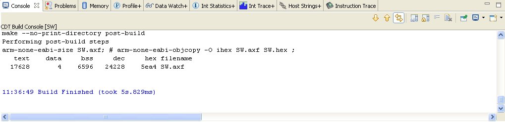
- To Flash the project you need to build it, from the menu go to Project -> Build All. The console window will display the compilation.
- Then click on the processor icon.

- LPC-Link 2
- Connect LPC-Link 2 with the pc
Note
LPC-Link 2 can draws a significative amount of current from the usb. The best solution is to connect LPC-Link 2 to a powered hub.
- If drivers are required choose the automatic sequence of installation
3. Connect LPC-Link 2 with the target with a cable the J4 LPC-Link connector to the CN3 connector of the Louvre board. Here the connection scheme:
| pin J4 | pin CN3 | Signal Names |
|---|---|---|
| 2 | 2 | JTAG_TMS_SWDIO |
| 4 | 4 | JTAG_TCLK_SWCLK |
| 10 | 1 | JTAG_RESET |
| 3 or 5 or 9 | 3 | GND |
- Open LPCXpresso and load the project then run->debug configurations, select debugger tab
- On emulator selection voice choose Redlink server
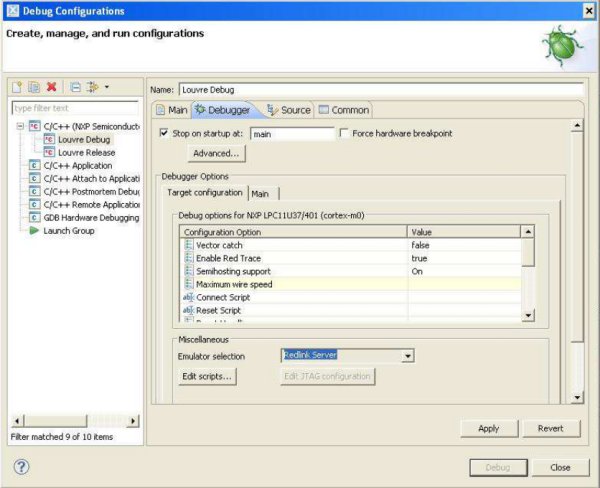
- Click Apply and Close buttons, then click on the processor icon:
Bootloader Details
The bootloader is the first program executed, located in the first two blocks of the flash memory (0x0000 - 0x1FFF) for a total size of 8K bytes. It controls the presence of a NFC segnal with a new valid application; if so, received data are written in flash. After, it calculates the validity of the CRC flash memory, if it is valid then copies the applicative interrupt vectors ram memory (0x10000000 - 0x100000bf) and launches it. If the application is not valid then it checks continuosly NFC signal waiting a new program to download.
Flash memory map:0000 00BF bootloader code vector table00C0 1FFB bootloader code1FFC 1FFF software versionRam memory map:0x10000000 0x100000BF applicative interrupt vectors table0x100000C0 bootloader/applicative ram memoryApplicative:Flash memory map:2000 2003 applicative checkusm (used by bootloader to verify the code)2004 2007 applicative lenght2008 200B applicative version200C 20BF applicative code vector table (will be copied in the ram memory)20C0 applicative codeRam memory map:0x10000000 0x100000BF applicative interrupt vectors table0x100000C0 ram memory
Important